Search the Community
Showing results for tags 'electronic components'.
-
What does TDA12156PS/N3/3 used for? I could not see which catalogue it is in. would like to know more the specification and functions about it. who can tell me? Thanks in advance.
-
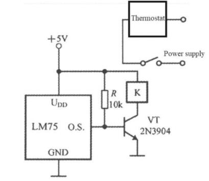
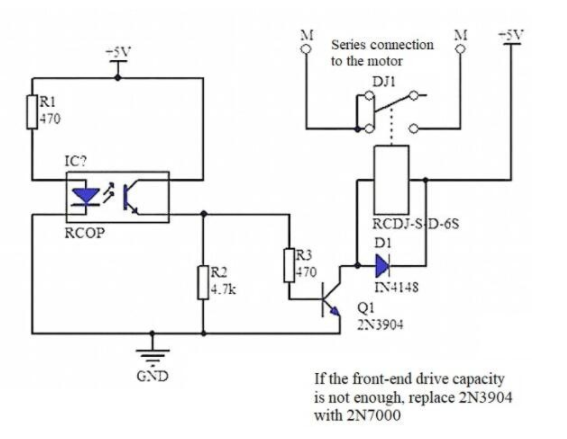
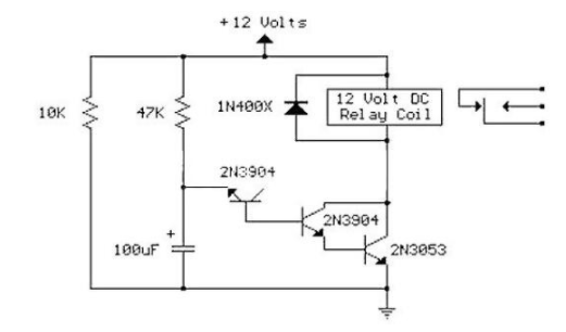
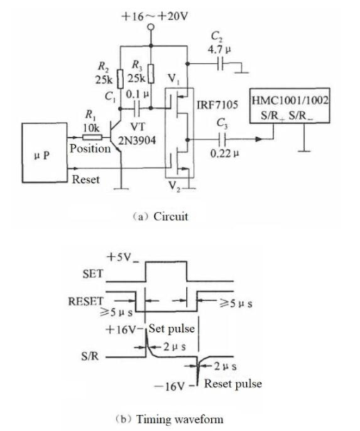
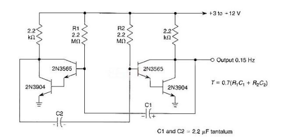
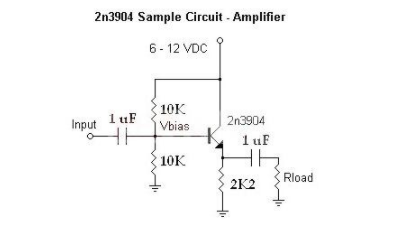
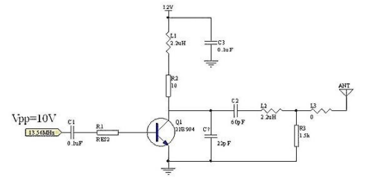
In this article, we have produced 7 simple 2N3904 circuits for electronic enthusiasts. These circuit diagrams are essentially beginner-friendly types. Hope the circuit diagrams are helpful to you.😀 Source: Apogeeweb Semiconductor Electronic 2N3904 Circuit Circuit 1: Thermostat controller composed of LM75 intelligent temperature sensor and 2N3904 transistor. Circuit 2 Circuit 3 Circuit 4 Circuit 5 Circuit 6: 2N3904 Sample Circuit-Amplifier Circuit 7:How to design a 13.56mhz sine wave power amplifier circuit with 2N3904
-
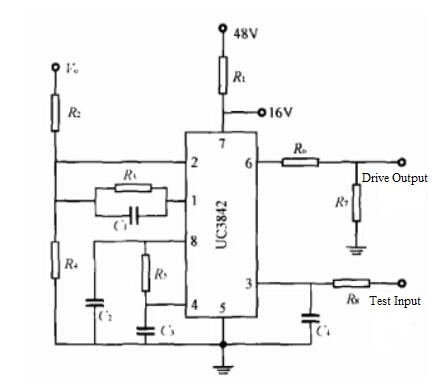
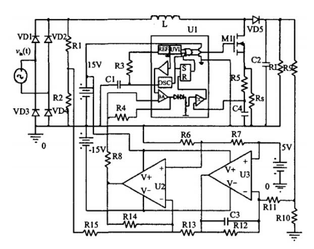
UC3842 is a fixed frequency current-mode PWM controller. This IC is specially designed for Off-Line and DC to DC converter applications with minimum external components. In the blog today, we'll have a further discussion about the application of UC3842 in the boost conversion circuit. Boost Conversion Circuit Overview Boost converters can reduce the output current and the capacitance and volume of the output filter capacitor under a certain output power, and are widely used in switching power supplies and electronic ballasts. Commonly used control methods are voltage feedback control and current feedback control. Current feedback control can force the inductor current to track the reference current signal, which has the advantage of fast response. When working in continuous current mode (CCM), the Boost converter needs to introduce multiple feedback methods. When working in discontinuous current mode (DCM), the converter automatically shapes the input current, and has a natural zero-current turn-on characteristic, requires a small inductance value, simple control, and is suitable for low-power applications. At present, there are many researches on the CCM mode of Boost conversion circuit, and many circuit models have been established, and gratifying research results have been obtained; the research on DCM mode is mainly DC/DC circuit, and the research on DCM mode in AC/DC circuit Very little. Based on the requirements of low-power switching power supply with low cost and high cost performance, this paper uses the universal UC3842 chip to design a Boost conversion circuit, analyzes the working characteristics and design points of the DCM mode, and simulates the rationality of the designed circuit verification. There are 2 circuit models of boost converter in DCM mode, named spectively as: Mathematical Model of DCM Working Mode and Working Conditions of DCM Mode. For detailed explanation to these two models>> DCM Circuit Design Based on UC3842 DCM Circuit Design Based on Adder The DCM-type Boost circuit includes two control loops, namely a voltage loop and a current loop. Its function is to eliminate the grid current spikes, so that the input current becomes a sinusoidal shape and is in phase with the input voltage. For a single switching cycle, the current in each switching cycle is required to be proportional to the input voltage. If for some reason the output voltage increases or the output current increases, the pulse width modulator will change the pulse width of the drive signal, that is, the duty cycle D, so that the average voltage or peak current after the chopping will decrease. So as to achieve the purpose of power factor correction. The DCM circuit schematic diagram based on the adder is shown in Figure below. The voltage outer loop uses an adder to replace the multiplier circuit. The feedback voltage on the grid side is used to ensure that the current signal is a sinusoidal signal, and the output feedback voltage is used to ensure that the output voltage is a constant value. The two are synthesized by the adder U2. The output signal is sent to the error amplifier in the UC3842 current loop, compared with a given reference voltage, and the comparison result is sent to the current measurement comparator. The peak current signal L(t) of the inductor in the main circuit is sent to the current measuring comparator at the same time, the comparison result of the two is sent to the R input of the RS latch in the PWM, the clock signal output by the internal oscillating circuit is sent to the S input end of the RS latch in the PWM, which works together to control the opening and closing of the switch tube M1. The follow-up simulation and analysis of DCM mode circuit>> Conclusion This text summarizes the Boost conversion circuit design scheme based on UC3842 chip. By analyzing the circuit of Boost converter in DCM mode, the circuit model of Boost converter in DCM mode is established, and the duty cycle change rule in this mode and the critical conditions for entering CCM mode from DCM mode are studied. Using the universal PWM modulator UC3842 chip, a Boost conversion circuit based on the principle of addition is designed, and the correctness of the conclusions obtained is verified by simulation software. The circuit simulation results show that the designed DCM circuit can meet the requirement of the inductor current to follow the voltage waveform completely and achieve the purpose of improving the power factor. This research provides design ideas for the development of low-cost low-power switching power supplies.
- 1 reply
-
- circuit design
- boost conversion
-
(and 4 more)
Tagged with:

