


DiyProjectLab
-
Posts
8 -
Joined
-
Last visited
Content Type
Profiles
Forums
Events
Posts posted by DiyProjectLab
-
-
- Sometimes there are some problems with your PCB designs, after you have a prototype, some of them go wrong, then you are upset that where the mistake has happened, for this problem you need a software that makes those mistakes. Show us
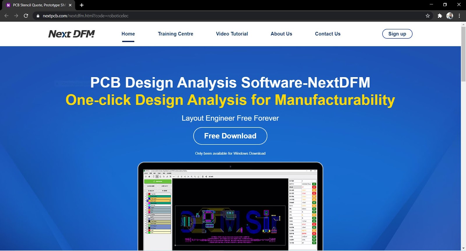
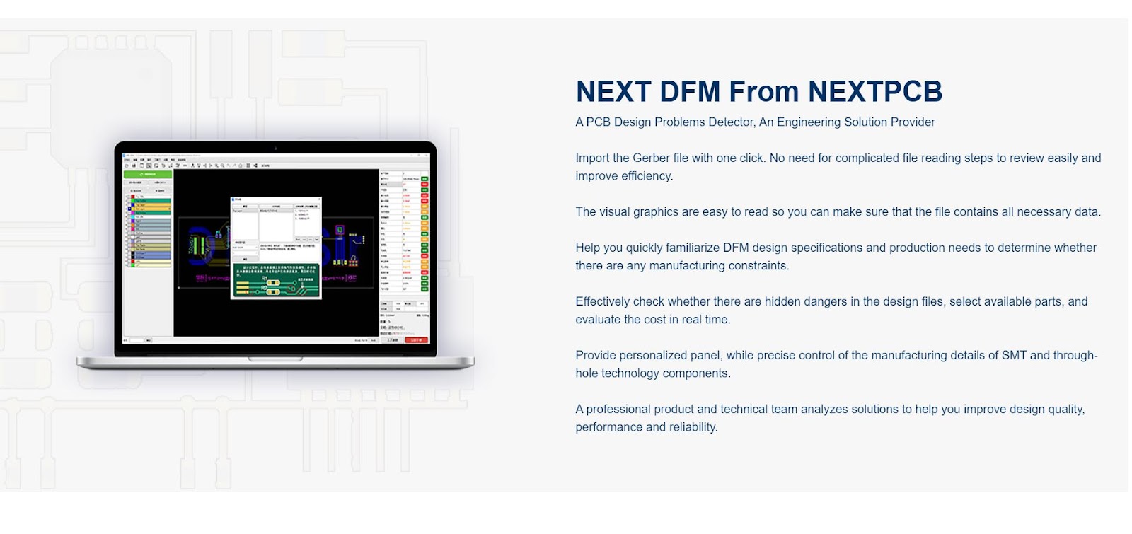
NextDFM is a PCB problem detector and engineering tool by NextPCB, one of the most professional PCB manufacturers in the world based in China. This article is for the review of the NextDFM software installation, features and benefits of this software. NextDFM is a simple software which can be learnt easily by a non regular PCB designer also. The UI created by them is very simple and PCB design analysis can be done in just a few clicks.
Installation of NextDFM software
Click on the below link to move to the homepage of the NextDFM website of NextPCB and you can find the home page similar to the below figure. Link for software download
Now to start downloading just signup if you are a new user of the website then click on the Free Download button and then just run it on your computer(Only windows OS version is available).
Features of the software
- Helps in making PCB design more standard.
- Identify the hazards of the design.
- Visual simulation of the PCB files.
- Instant quote and billing options.
Interface of the NEXT DFM Software
http://www.diyprojectslab.com/wp-content/uploads/2021/01/Capture-1024x475.jpg Click on Free download
http://www.diyprojectslab.com/wp-content/uploads/2021/01/5.jpg Select Destination File location for all Data
http://www.diyprojectslab.com/wp-content/uploads/2021/01/6.jpg select Start menu folder- http://www.diyprojectslab.com/wp-content/uploads/2021/01/7.jpg
It is quite easy to install it. Like all other software.
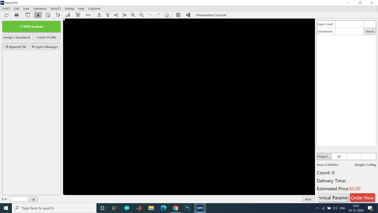
After installing it, after opening it, you will get a view as shown below.
http://www.diyprojectslab.com/wp-content/uploads/2021/01/g-2.jpgFirst you have to login before using it
- http://www.diyprojectslab.com/wp-content/uploads/2021/01/zip.jpg
- http://www.diyprojectslab.com/wp-content/uploads/2021/01/gerb.jpg
Extract PCB Gerber zip file
- http://www.diyprojectslab.com/wp-content/uploads/2021/01/next-1024x547.jpg
http://www.diyprojectslab.com/wp-content/uploads/2021/01/hg-1-1024x547.jpgNow you upload your gerber file।
http://www.diyprojectslab.com/wp-content/uploads/2021/01/pcb-1024x546.jpgHere you can see that my design
The above image is the starting window of the NEXT DFM Software then click on the file and then open the gerber file of your PCB design by selecting and uploading all the layer files. I have uploaded a gerber file of IR Sensor for the demo.
Then you can select and deselect any layer of your design by simply clicking on the layers present on the left most window.
http://www.diyprojectslab.com/wp-content/uploads/2021/01/tf-1024x640.jpgNow you can also choose the colours as per your wish we have choice of green, blue, black, red, yellow and white colours and also choice of the surface finish and silkscreen options as a reviewer I can say that this is a great option to customize your PCB colour and other physical properties along with the visuals on the middle window screen.
http://www.diyprojectslab.com/wp-content/uploads/2021/01/IMG_20210109_175630.jpgThe special thing about this software is that you can order your PCB from this.
This is how it looks after changing the colour of the PCB to blue. This tool helps you to visualize your PCB in the best way. On the Right top you will be having details about the number of layers in the PCB and its dimensions. On the right bottom you find the estimated price and the delivery time you can order directly by clicking on the Order now button.
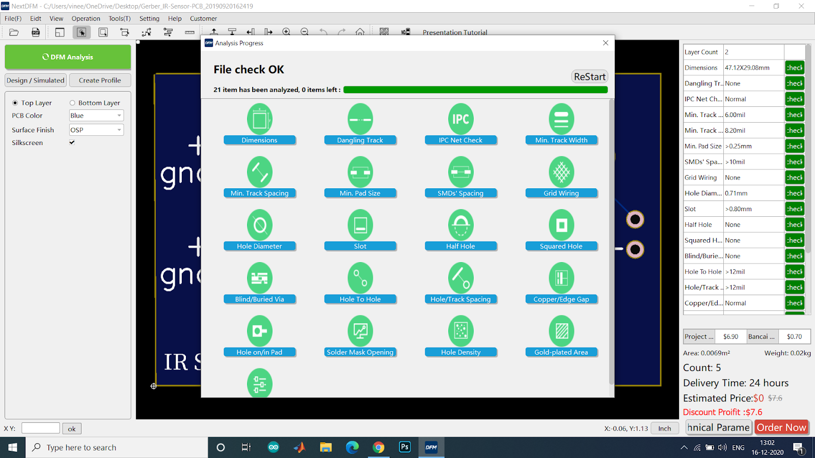
On clicking on the DFM Analysis button on the left window the software will analyze the design of the PCB automatically with the 21 parameter error check and suggest to you if any errors are present it is the most important and striking feature of this software.
So download this software and tell us the features liked by you in this software and share this article..
-
- Sometimes there are some problems with your PCB designs, after you have a prototype, some of them go wrong, then you are upset that where the mistake has happened, for this problem you need a software that makes those mistakes. Show us
NextDFM is a PCB problem detector and engineering tool by NextPCB, one of the most professional PCB manufacturers in the world based in China. This article is for the review of the NextDFM software installation, features and benefits of this software. NextDFM is a simple software which can be learnt easily by a non regular PCB designer also. The UI created by them is very simple and PCB design analysis can be done in just a few clicks.
Installation of NextDFM software
Click on the below link to move to the homepage of the NextDFM website of NextPCB and you can find the home page similar to the below figure. Link for software download
Now to start downloading just signup if you are a new user of the website then click on the Free Download button and then just run it on your computer(Only windows OS version is available).
Features of the software
- Helps in making PCB design more standard.
- Identify the hazards of the design.
- Visual simulation of the PCB files.
- Instant quote and billing options.
Interface of the NEXT DFM Software
http://www.diyprojectslab.com/wp-content/uploads/2021/01/Capture-1024x475.jpg Click on Free download
http://www.diyprojectslab.com/wp-content/uploads/2021/01/5.jpg Select Destination File location for all Data
http://www.diyprojectslab.com/wp-content/uploads/2021/01/6.jpg select Start menu folder- http://www.diyprojectslab.com/wp-content/uploads/2021/01/7.jpg
It is quite easy to install it. Like all other software.
After installing it, after opening it, you will get a view as shown below.
http://www.diyprojectslab.com/wp-content/uploads/2021/01/g-2.jpgFirst you have to login before using it
- http://www.diyprojectslab.com/wp-content/uploads/2021/01/zip.jpg
- http://www.diyprojectslab.com/wp-content/uploads/2021/01/gerb.jpg
Extract PCB Gerber zip file
- http://www.diyprojectslab.com/wp-content/uploads/2021/01/next-1024x547.jpg
http://www.diyprojectslab.com/wp-content/uploads/2021/01/hg-1-1024x547.jpgNow you upload your gerber file।
http://www.diyprojectslab.com/wp-content/uploads/2021/01/pcb-1024x546.jpgHere you can see that my design
The above image is the starting window of the NEXT DFM Software then click on the file and then open the gerber file of your PCB design by selecting and uploading all the layer files. I have uploaded a gerber file of IR Sensor for the demo.
Then you can select and deselect any layer of your design by simply clicking on the layers present on the left most window.
http://www.diyprojectslab.com/wp-content/uploads/2021/01/tf-1024x640.jpgNow you can also choose the colours as per your wish we have choice of green, blue, black, red, yellow and white colours and also choice of the surface finish and silkscreen options as a reviewer I can say that this is a great option to customize your PCB colour and other physical properties along with the visuals on the middle window screen.
http://www.diyprojectslab.com/wp-content/uploads/2021/01/IMG_20210109_175630.jpgThe special thing about this software is that you can order your PCB from this.
This is how it looks after changing the colour of the PCB to blue. This tool helps you to visualize your PCB in the best way. On the Right top you will be having details about the number of layers in the PCB and its dimensions. On the right bottom you find the estimated price and the delivery time you can order directly by clicking on the Order now button.
On clicking on the DFM Analysis button on the left window the software will analyze the design of the PCB automatically with the 21 parameter error check and suggest to you if any errors are present it is the most important and striking feature of this software.
So download this software and tell us the features liked by you in this software and share this article..
-
Story
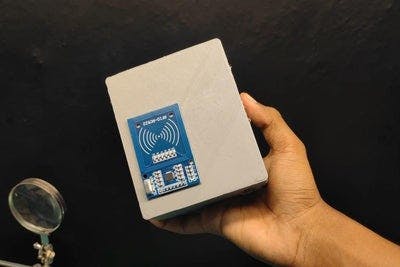
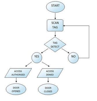
Hii friends Today I'll Show You How To Make RFID Door Lock System Using Arduino Nano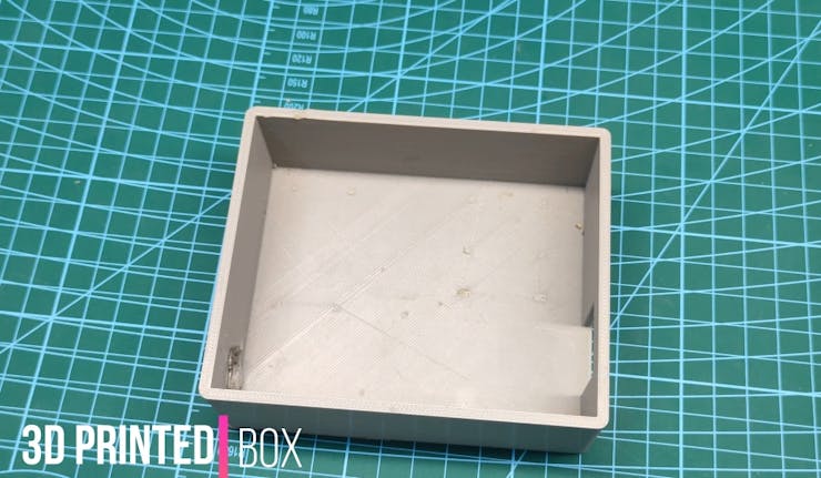 1 / 8
1 / 8The arduino based RFID door lock system is secure and responsive as compared to other systems. With the use of arduino, it becomes much easy to design. Program a code and upload it to arduino just like a plug and play device. It is simple and cost efficient project and can be used as a basic access control mechanism. Their main advantage is contactless communication and RFID tags can work in any environmental conditions.
Supplies:You'll nees Some Componenets
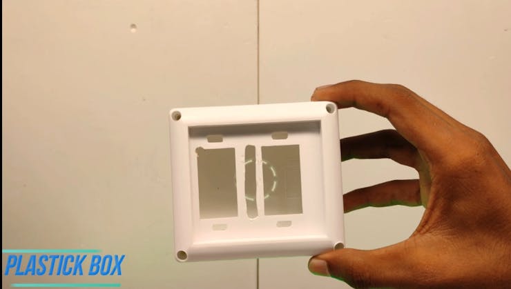
- Plastic Box
- Rfid Module
- 12V solenoid Lock
- Arduino nano
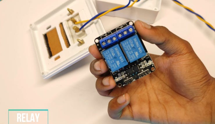
- 1ch Relay Module
- Some Jumper Wire
- 5V TO 12v CONVERTOR
- DC Socket
- 5V adapter
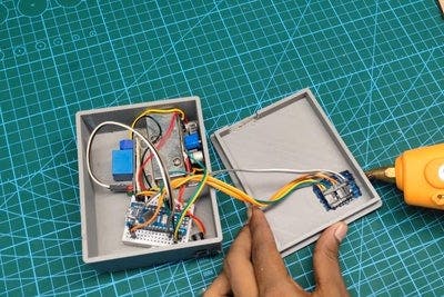
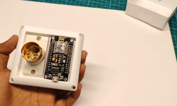
Step 1: Solder RFID Module
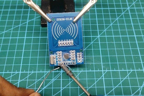
Solder the mail header with Rafid
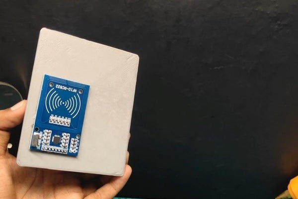
Step 2: Stick RFID in the Lid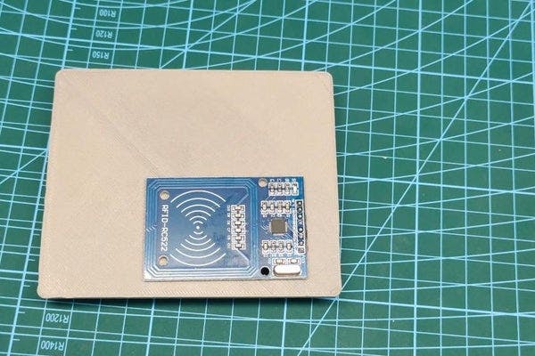
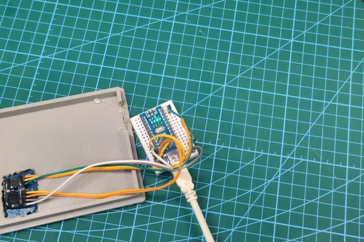
Step 3: Connections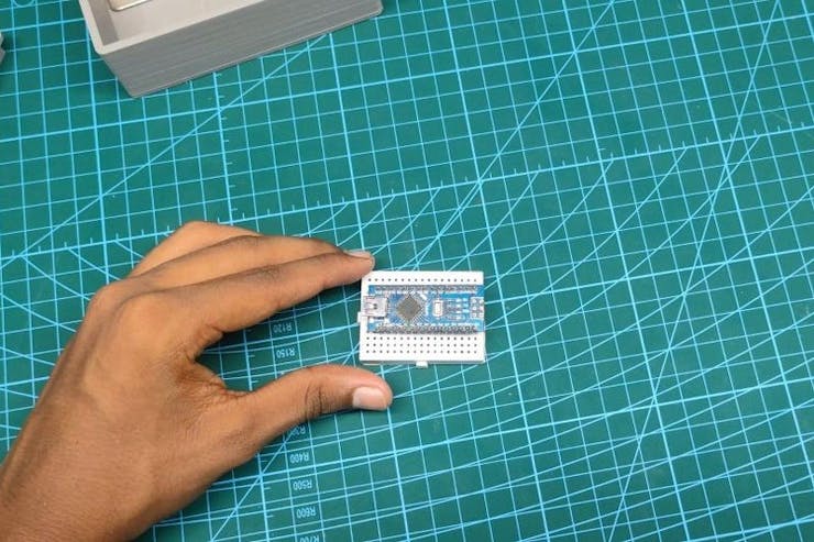
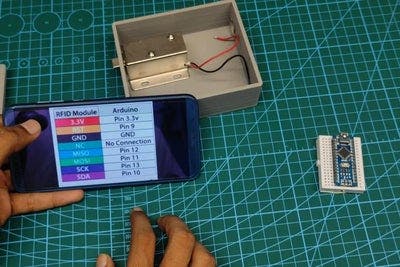
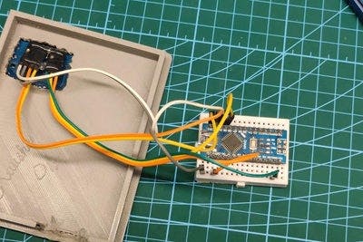
Combine all the components with the arduino as shown in the Pic
ARDUINO to RFID reader
pin 11 to MISO
pin 12 to MOSI
pin 13 to SCK
pin 10 to NSS
pin 9 to RST
These were the connection from Arduino to RFID reader
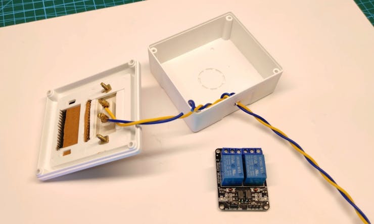
Relay Module Arduino Nano
Vcc 5v
GND GND
In1 D3
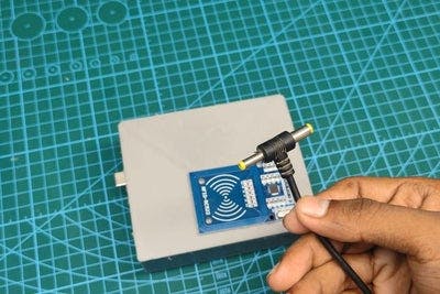
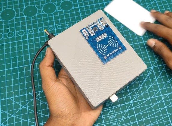
Step 4: Keep All the Components in the Box Properly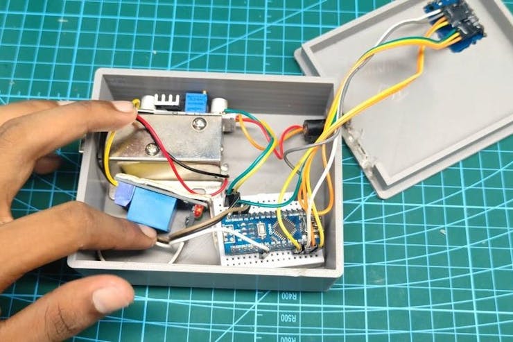
Step 5: Let's Programming & Flowchart
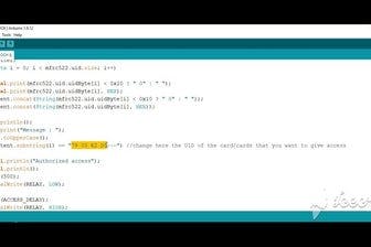
Attachments📷source_code.ino (1).txt
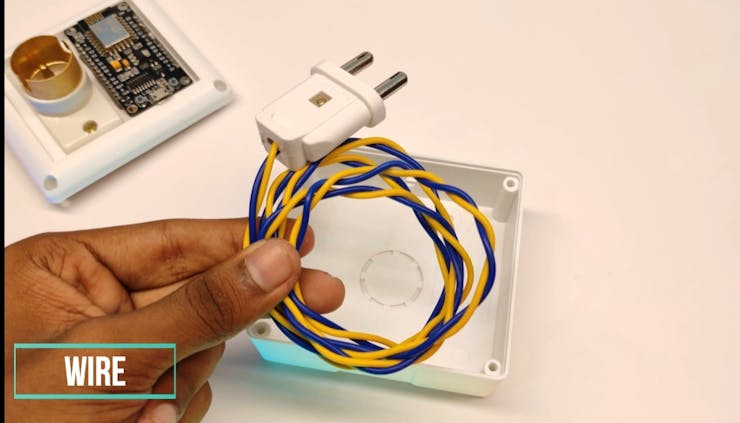
Step 6: 5V Power Supply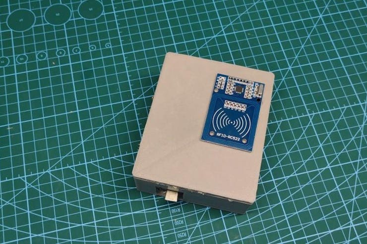
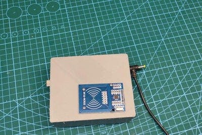
Step 7: Complete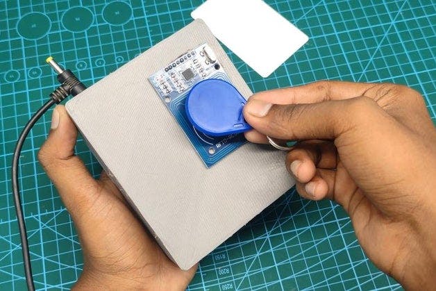
 ht
ht
Step 10: Nextpcb
As per my circuit diagram, I have made a PCB layout and order it on NEXTPCBI have received this PCB after 7 days, the PCB quality is very good and also the price of PCB is also low
if you don't make your PCBs yourself, where do you make them?Personally, I do not have the space and the courage (nor the skill) to do them my self.For SF, I turn to Util-Pocket, because I find that the quality is excellent for the price. For the DF (with metallic holes), I tried several companies, all of which do a good job, but it costs a lot.This time I addressed myself here. I had 3 circuits to do, totaling an average surface of 49 cm2.When I saw that the minimum quantity to order was 5 PCBs, I continued my order out of curiosity, just to see the quote. And when I saw the asking price, I placed the order. Nextpcb
-
Story
Subscribe For MoreHii Friends Welcome Back 🤗
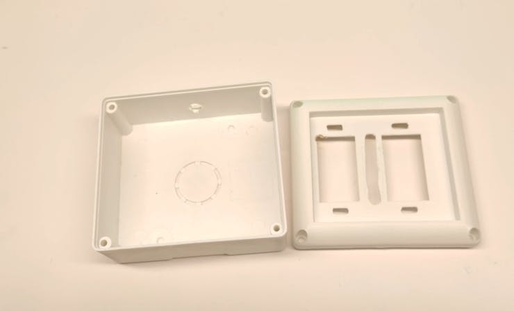
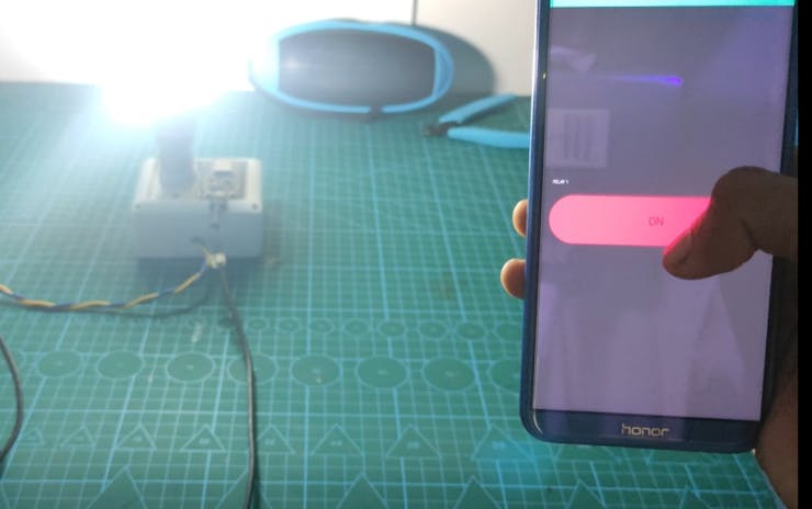
Today I'll Show You How To make Simple Home automation System
So Let's Make It
You I'll Need Some Componenets For this

 5 / 5
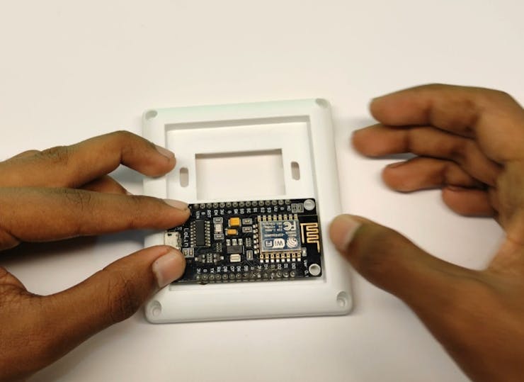
5 / 51. Plastic Box
2. Nodemcu
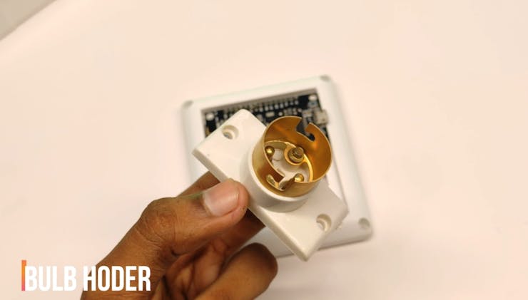
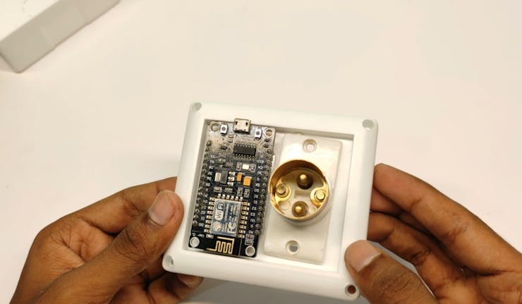
3. Bulb Holder
4. Wire
5. Relay Module
 1 / 3
1 / 3Fix the Nodemcu in Box
 2 / 3
2 / 3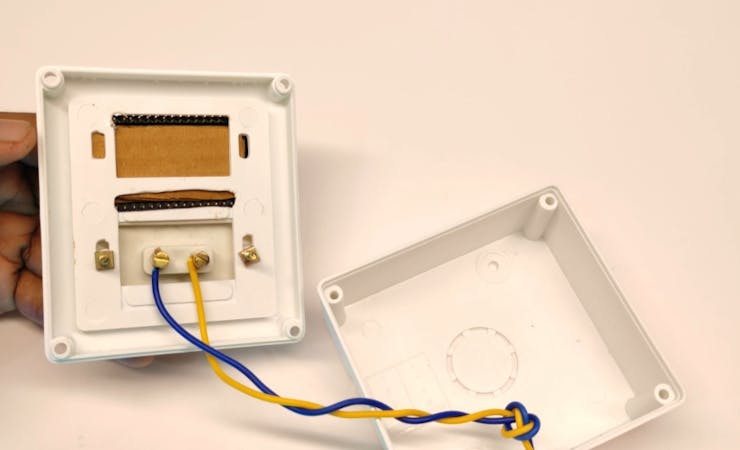
 3 / 3
3 / 3 1 / 2 • Connect Wire To Holder the Cut A Wire
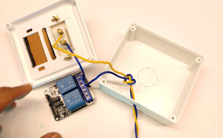
 2 / 2
2 / 2Connect the Cutting Wire In Relay
_4wL99D0224.jpeg?auto=compress%2Cformat&w=740&h=555&fit=max) Like This
Like This
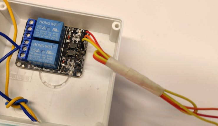
Connection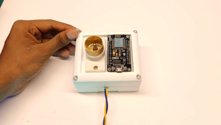
 4 / 4
4 / 4
Relay NodemcuGND GND
VCC 5v
IN1 D1
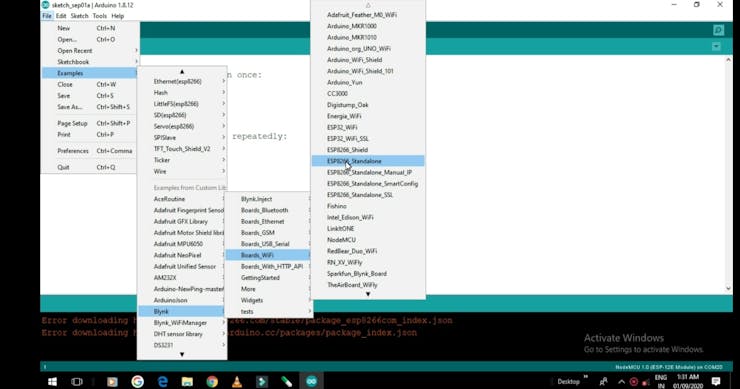
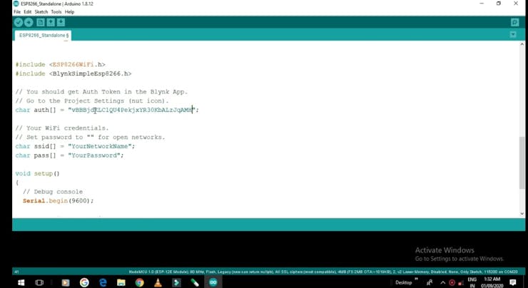
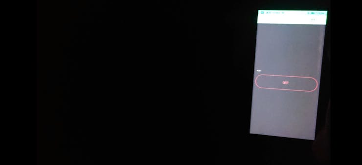
Let's Programming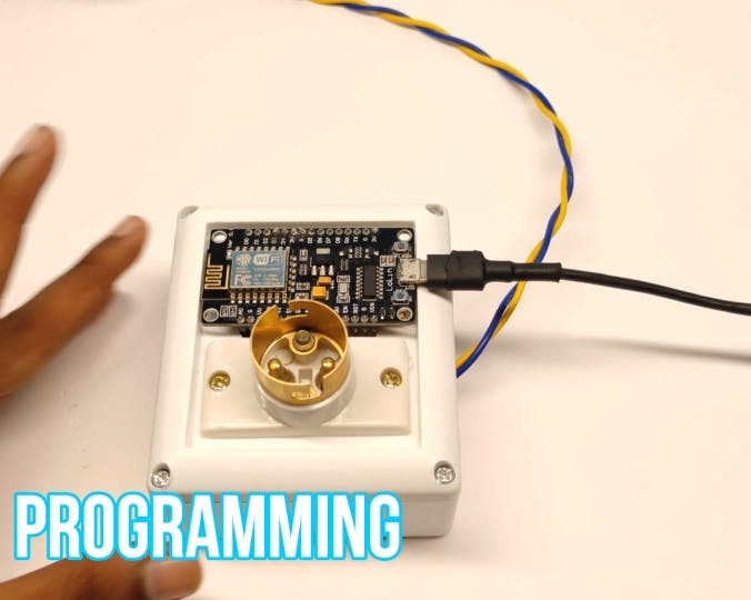
 2 / 3
2 / 31st Install The Blynk Libraries
And goto EXAMPLE - BLYNK -BLYNK WIFI - ESP8266 Standalone
Then Change your SSID, PASSWORD And Authorization Code
Then upload Your code
 4 / 5
4 / 5Nextpcb
_BRhvcj9ZIK.jpeg?auto=compress%2Cformat&w=740&h=555&fit=max) For Next Project
For Next ProjectThanks for NextPCB sponsor this project. For New Customer, Your First Order Will Be Free. http://www.nextpcb.comNextPCB is a high-quality PCB Manufacturer in Shenzhen China. With professional PCB manufacturing capabilities, for each file of our customer will be double-checked by more than 10 years PCB engineers. PCB materials are certified by ISO9001, UL; We handle the whole process including PCB manufacturing, PCB assembly, testing, and final shipment. We are capable of assembling BGA, Micro-BGA, QFN and other leadless package parts. We also have an online parts shop, you can choose any parts if you needit.
Video For Full Tutorial👍🏻👍🏻👍🏻
-
Hii Friends Today I'll Show You How To Make Simple DIY Arc Reactor Using WemosD1
SO LET'S Make It🔥Please Subscribe My Channel For More
Supplies:
Hardware:
WemosD1
Ws2812b RGB Led Strip
3D printed Box
Some Wires
5V Adapter
: Buying these from local shops would be a better
Software
:- Arduino IDE
BlynkTipQuestionCommentStep 1: Step 1: WS2812B LED (Neopixe L) Strips Are Individually Addressable LED Strips


WS2812B LED (Neopixel) Strips are individually addressable LED strips. These are awesome tools. The ability to program each LED individually using only one data line is amazing. The pad on the strips allow you to solder directly to this semi-flexible PCB, but I find that a little cumbersome. Here's how I make modular hookups for these types of strips or the older 4-pin style of addressable strips.TipQuestionCommentStep 2: Print Your Arc Reactor With 3D Printer


I made this using 3D printer
TipQuestionCommentStep 3: Put the Wemos D1 in Arc Reactor


I have used Wemos D1 to make it because it is very small and also works great.
You can also use Nodamcu
TipQuestionCommentStep 4: RGB STRIP LED


I used this W2812b RGB Strip led in it
I would advise you to use the same as they are very good
Now you put the strip led in a REACTOR
As shown in the image
Connections :-
Vcc to 5V
GND to GND
Din pin to D3TipQuestionCommentStep 5: Put All Part in Arc Reactor


Now paste all the parts into it
TipQuestionCommentStep 6: Let's Programming


Download Libraries
First we will need the adafruit neopixel library to control the LEDs. It can be found in the libraries manager, just search for 'adafruit neopixel' and select the one shown and install it....
Then to download the board definitions, open prefrences and paste ..
http://arduino.esp8266.com/stable/package_esp8266c... into the 'additional board URLs' box. Then open boards manager and search for 'esp8266' it should be the first one, click on it and install it....
Code
Create a new sketch and name it 'neopixels on WemosD1 with blynk' (or something that you're going to remember). Paste in the code. Change 'yourAuthCode' to the auth code for your project. (found in the 'nut' icon in blynk app) Change your wifi name and password to those of your network. Set the number of neopixels to the length of your strip. Plug your MCU into your computer, select Wemos D1 from the board menu in the ide, select the COM port and baud rate(115200) but ignore all the rest, it should be pre-configured.
Then upload!!TipQuestionCommentStep 7: BLYNK


Install blynk app from app store or play store.
Create a New Project in BLYNK app.Write Project Name and Select Wemos or WemosD1 from dropdown.An AUTH token will be sent to your registered email, note this down.Tap on the screen and add a ZERGBA WIDGET on screen..
Note: This will change colors only over WIFI not over internet.TipQuestionCommentStep 8: Finished


Thanks For watch
❤️
If you have any doubt, please ask in the inbox❤️TipQuestionCommentStep 9: Thanks Nextpcb for Sponsoship


If you don't make your PCBs yourself, where do you make them?Personally, I do not have the space and the courage (nor the skill) to do them myself.For SF, I turn to Util-Pocket, because I find that the quality is excellent for the price.For the DF (with metallic holes), I tried several companies, all of which do a good job, but it costs a lot.This time I addressed myself here. I had 3 circuits to do, totaling an average surface of 49 cm2.When I saw that the minimum quantity to order was 5 PCBs, I continued my order out of curiosity, just to see the quote.And when I saw the asking price, I placed the order.NEXTPCB
-
DIY Rainbow Eclipse Wall Light
Introduction: DIY Rainbow Eclipse Wall Light


Hii Friends Today I'll Show You How To Make Simple DIY Eclipse Wall Light Using ESP8266
SO LET'S Make It🔥
I created this project after I was inspired by smartphone controlled neopixels in a friends house but his were shop-bought. I thought "how hard can it be to make my own, it would be much cheaper too!"
(✯ᴗ✯) (✯ᴗ✯)
Supplies:
Hardware:
Ws2812b RGB Led Strip
Wires
: Buying these from local shops would be a better
Software:
Arduino IDE
BLYNK App
TipQuestionCommentStep 1: WS2812B LED (Neopixel) Strips Are Individually Addressable LED Strips


WS2812B LED (Neopixel) Strips are individually addressable LED strips. These are awesome tools. The ability to program each LED individually using only one data line is amazing. The pad on the strips allow you to solder directly to this semi-flexible PCB, but I find that a little cumbersome. Here's how I make modular hookups for these types of strips or the older 4-pin style of addressable strips.
TipQuestionCommentStep 2: Print Your Plate With 3D Printer


I made this plate using 3D printer
If you don't have a 3D printer, don't worry, you can make it without a 3D printer.
You will need a box lid
And you can use it to make it 😞
You can Download 3d Printing File From Here.
- DESIGN CREDIT :- Jason Coon
TipQuestionCommentStep 3: RGB STRIP LED


I used this W2812b RGB Strip led in it
I would advise you to use the same as they are very good
Now you put the strip led in a plate
As shown in the image
TipQuestionCommentStep 4: Connect the RGB Led With Esp8266


I have used ESP8266 in it, if you also have Wemos D1, then we can use it
Connections :-
RGB LED ESP8266
DIN Pin D3
GND GND
VCC 3.3v
TipQuestionCommentStep 5: Upload Code in ESP8266


Download Libraries
First we will need the adafruit neopixel library to control the LEDs. It can be found in the libraries manager, just search for 'adafruit neopixel' and select the one shown and install it....
Then to download the board definitions, open prefrences and paste ..http://arduino.esp8266.com/stable/package_esp8266c... into the 'additional board URLs' box. Then open boards manager and search for 'esp8266' it should be the first one, click on it and install it....
Code
Create a new sketch and name it 'neopixels on esp8266 with blynk' (or something that you're going to remember). Paste in the code. Change 'yourAuthCode' to the auth code for your project. (found in the 'nut' icon in blynk app) Change your wifi name and password to those of your network. Set the number of neopixels to the length of your strip. Plug your MCU into your computer, select MCU from the board menu in the ide, select the COM port and baud rate(115200) but ignore all the rest, it should be pre-configured.Then upload!!
Attachments
TipQuestionCommentStep 6: Blynk


Install blynk app from app store or play store.
Create a New Project in BLYNK app.Write Project Name and Select ESP8266 or NodeMCU from dropdown.An AUTH token will be sent to your registered email, note this down.Tap on the screen and add a ZERGBA WIDGET on screen..
Note: This will change colors only over WIFI not over internet.TipQuestionCommentStep 7: Upload the Code to NodeMCU and Play

Upload the code to your NodeMCU or ESP8266 and device will be displayed online on your BLYNK app.
Click Play button on top right of your app and start changing colors of your light. Oh yeah!
TipQuestionCommentStep 8: Finished


Small (5.25" / 133.35mm) clock and art display built with 60 RGB LEDs, controlled with an ESP8266 using the FastLED library.
Fully open-source, and programmable over Wi-Fi or micro USB cable.
If there is any problem then you can ask me in the comment
(θ‿θ)
TipQuestionCommentStep 9: : Thanks Nextpcb for Sponsoship

If you don't make your PCBs yourself, where do you make them?Personally, I do not have the space and the courage (nor the skill) to do them myself.For SF, I turn to Util-Pocket, because I find that the quality is excellent for the price.For the DF (with metallic holes), I tried several companies, all of which do a good job, but it costs a lot.This time I addressed myself here. I had 3 circuits to do, totaling an average surface of 49 cm2.When I saw that the minimum quantity to order was 5 PCBs, I continued my order out of curiosity, just to see the quote.And when I saw the asking price, I placed the order.NEXTPCB -

In this project I will be showing you How To Make DIY Music Relative Led Strip Light Using Arduino Nano
Let’s get started!
You Will Need Some Componenets For Make This Project
Arduino Nano
RGB strip Light
Sound Sensor
Adapter 5V
Cable.jpeg.396482a99ca5e26e48f7cfd5200e9efa.jpeg)
.jpeg.80fd124cc584f9f974816f4048ddd595.jpeg)

Nextdfm
in Electronic Projects
Posted
NextDFM is a PCB problem detector and engineering tool by NextPCB, one of the most professional PCB manufacturers in the world based in China. This article is for the review of the NextDFM software installation, features and benefits of this software. NextDFM is a simple software which can be learnt easily by a non regular PCB designer also. The UI created by them is very simple and PCB design analysis can be done in just a few clicks.
Installation of NextDFM software
Click on the below link to move to the homepage of the NextDFM website of NextPCB and you can find the home page similar to the below figure. Link for software download
Interface of the NEXT DFM Software
http://www.diyprojectslab.com/wp-content/uploads/2021/01/5.jpg Select Destination File location for all Data
http://www.diyprojectslab.com/wp-content/uploads/2021/01/6.jpg select Start menu folder-
http://www.diyprojectslab.com/wp-content/uploads/2021/01/7.jpg
http://www.diyprojectslab.com/wp-content/uploads/2021/01/8-2.jpg Click on install and Install it http://www.diyprojectslab.com/wp-content/uploads/2021/01/9.jpg Installing http://www.diyprojectslab.com/wp-content/uploads/2021/01/10.jpgIt is quite easy to install it. Like all other software.
After installing it, after opening it, you will get a view as shown below.
http://www.diyprojectslab.com/wp-content/uploads/2021/01/g-2.jpgFirst you have to login before using it
Extract PCB Gerber zip file
http://www.diyprojectslab.com/wp-content/uploads/2021/01/hg-1-1024x547.jpgNow you upload your gerber file।
http://www.diyprojectslab.com/wp-content/uploads/2021/01/pcb-1024x546.jpgHere you can see that my design
The above image is the starting window of the NEXT DFM Software then click on the file and then open the gerber file of your PCB design by selecting and uploading all the layer files. I have uploaded a gerber file of IR Sensor for the demo.
Then you can select and deselect any layer of your design by simply clicking on the layers present on the left most window.
http://www.diyprojectslab.com/wp-content/uploads/2021/01/tf-1024x640.jpg
Now you can also choose the colours as per your wish we have choice of green, blue, black, red, yellow and white colours and also choice of the surface finish and silkscreen options as a reviewer I can say that this is a great option to customize your PCB colour and other physical properties along with the visuals on the middle window screen.
http://www.diyprojectslab.com/wp-content/uploads/2021/01/IMG_20210109_175630.jpg
The special thing about this software is that you can order your PCB from this.
This is how it looks after changing the colour of the PCB to blue. This tool helps you to visualize your PCB in the best way. On the Right top you will be having details about the number of layers in the PCB and its dimensions. On the right bottom you find the estimated price and the delivery time you can order directly by clicking on the Order now button.
On clicking on the DFM Analysis button on the left window the software will analyze the design of the PCB automatically with the 21 parameter error check and suggest to you if any errors are present it is the most important and striking feature of this software.
So download this software and tell us the features liked by you in this software and share this article..