Jump to content

Search the Community

Showing results for tags 'electronics'.

  • Search By Tags

    Type tags separated by commas.
  • Search By Author

Content Type


Forums

  • Electronics Design
    • Electronic Projects
    • Electronics Theory
    • Power Electronics
    • Electronic Components
    • Spice Simulation
    • Datasheets
    • General Electronic Discussion
  • Digital Electronics & Microcontrollers
    • Microcontroller Projects / Programming
    • Arduino
  • PCB Design - Hardware
    • PCB Design Software / Questions
    • Mechanical Constructions
  • Others
    • Announcements
    • Feedback / Comments
    • Sell / Buy Electronics
    • Job Offer / Requests

Find results in...

Find results that contain...


Date Created

  • Start

    End


Last Updated

  • Start

    End


Filter by number of...

Joined

  • Start

    End


Group


AIM


MSN


Website URL


ICQ


Yahoo


Jabber


Skype


Location


Interests

Found 4 results

  1. The TOP250YN is a high-efficiency, integrated power switch designed for use in isolated and non-isolated power supply designs. It is part of the TOPSwitch family of controllers, which are known for their performance, ease of use, and reliability. This device can operate in various modes like flyback, forward, or buck converters, which makes it adaptable to a wide range of power supply applications. The TOP250YN is especially well-suited for building power supplies with output voltages ranging from 5V to 15V, which are commonly used in low-power electronics. In this project, we’ll be designing a 12V output power supply, ideal for powering devices that require a stable, regulated 12V DC input. Materials and Components Required Before diving into the step-by-step guide, let's first look at the list of components you'll need to build the 12V power supply using the TOP250YN. 1. TOP250YN Integrated Circuit – The heart of the power supply, responsible for controlling the switch-mode operation. 2. Transformer – A high-frequency transformer suitable for use with the flyback topology to step down the voltage to a safe level. 3. Input Capacitor (e.g., 100µF, 400V) – To smooth out the AC input signal. 4. Output Capacitor (e.g., 470µF, 25V) – To filter the output and stabilize the DC voltage. 5. Diode (e.g., 1N4007) – Used for rectifying the AC signal from the transformer. 6. Inductor (e.g., 100µH) – To filter high-frequency switching noise and smooth the output. 7. Resistors – Used for feedback control and regulating the output voltage. 8. Feedback Capacitor – To stabilize the feedback loop and improve performance. 9. Heat Sink – To prevent the TOP250YN from overheating during operation. 10. Bridge Rectifier – If using an AC input, the bridge rectifier is necessary to convert AC to DC. 11. Input Fuse – A fuse for safety to protect the power supply from overcurrent. 12. PCB (Printed Circuit Board) – A custom or pre-designed PCB to mount the components securely. 13. Miscellaneous – Connectors, wires, soldering supplies, and enclosures. Design Overview In this project, we'll build a flyback power supply based on the TOP250YN. The flyback topology is popular in many SMPS designs because of its simplicity, efficiency, and ability to provide galvanic isolation between the input and output. The power supply will have an input voltage range from 90V to 265V AC and output 12V DC with a maximum output power of around 10W. This is suitable for low-power applications such as powering sensors, microcontrollers, or small audio amplifiers. Step-by-Step Build Step 1: Preparing the Transformer The first step in the design process is to choose a suitable transformer. For a flyback design using the TOP250YN, you’ll need a transformer with a primary winding rated for the input voltage range (90-265V AC) and a secondary winding to output the desired 12V DC. The transformer should also have the appropriate turns ratio, typically in the range of 1:8 or 1:10, depending on the desired output current and voltage. The secondary side will step down the AC voltage, which will then be rectified and filtered to produce a smooth DC output. Mount the transformer securely on the PCB or in an appropriate casing, ensuring that the primary winding is connected to the AC input and the secondary winding will provide the low-voltage output. Step 2: Installing the TOP250YN IC The TOP250YN is the heart of the power supply, controlling the switch-mode operation of the flyback transformer. To install the TOP250YN, place it in the designated IC footprint on the PCB. The IC has an integrated high-voltage MOSFET and feedback circuitry that simplifies the design of the power supply. Connect the following pins of the TOP250YN to the appropriate components: ● Pin 1 (Drain): Connect this to the primary side of the transformer and the high-voltage input. ● Pin 2 (Source): Connect this to the ground (common) reference for the circuit. ● Pin 3 (Feedback): This is the feedback input that will connect to a resistor network, which provides feedback from the output to regulate the voltage. ● Pin 4 (VDD): Connect this to the output of the auxiliary power winding of the transformer (usually 12V or lower) to supply the IC. ● Pin 5 (GND): Ground reference for the IC. ● Pin 6 (GND/Secondary): Connect this to the secondary side of the transformer. Step 3: Setting Up the Rectification Circuit Once the AC input is stepped down by the transformer, the next step is to rectify it into DC. To do this, you will need a diode, such as the 1N4007, placed between the secondary winding of the transformer and the output capacitor. This diode will allow current to flow in one direction only, converting the AC signal into DC. The output capacitor will smooth the rectified signal, removing the ripple and providing a stable DC voltage. For this project, a 470µF capacitor with a voltage rating of at least 25V will suffice for the output stage. Step 4: Feedback Circuit for Regulation The TOP250YN uses a feedback mechanism to regulate the output voltage. You will need a resistor divider network connected to the feedback pin of the IC. The resistors in this network set the output voltage by monitoring the voltage at the output and feeding this information back to the IC. A small capacitor (e.g., 100nF) should be placed in parallel with the resistor network to stabilize the feedback loop and improve the performance of the power supply. Step 5: Adding Protection Components For the safety and longevity of your power supply, it is crucial to add protective components: 1. Input Fuse: Place a fuse in the AC input line to protect the circuit in case of a short circuit or overcurrent situation. Choose a fuse rated slightly above the maximum current draw of the power supply. 2. Heat Sink: Attach a heat sink to the TOP250YN to dissipate any heat generated during operation. Ensure that the heat sink is securely mounted and provides adequate thermal dissipation. 3. Overcurrent Protection: Consider adding an overcurrent protection circuit, such as a current sensing resistor, to prevent the power supply from delivering excessive current to the load. Step 6: Testing the Power Supply Before you connect the power supply to any critical load, perform the following tests: 1. Verify the Input Voltage: Measure the AC input to ensure it is within the recommended range (90V-265V AC). 2. Check the Output Voltage: With the power supply connected, measure the DC output voltage. It should be stable at around 12V, with minimal ripple. 3. Load Testing: Connect a small resistive load (e.g., a 12V LED strip or a suitable electronic device) to the output and monitor the output voltage under load. Ensure the voltage remains stable and the power supply does not overheat. Step 7: Enclosure and Final Assembly Once you’re confident that the power supply is working correctly, it’s time to mount it in a protective enclosure. A metal case is recommended for proper heat dissipation and safety. Ensure that the enclosure provides sufficient ventilation for the transformer and the IC. Secure the PCB inside the enclosure, making sure all connections are insulated and that there is no risk of short circuits. Finally, install the AC input connector and output terminals, ensuring that all connections are secure and that the power supply is safe to operate. Conclusion Building a high-efficiency power supply using the TOP250YN is an excellent project for those looking to explore switch-mode power supplies. By following the steps outlined in this guide, you will learn how to design and build a reliable and energy-efficient 12V DC power supply suitable for a wide range of low-power electronics. The TOP250YN’s integrated design simplifies the process, while still allowing for the flexibility to experiment and customize the power supply to your specific needs. This project not only introduces you to the basics of SMPS design but also gives you a practical, functional piece of equipment that can be used in various electronic applications. Whether you’re powering microcontrollers, sensors, or small motors, this power supply will serve as a valuable addition to your DIY electronics toolkit.
  2. The light comes on when my washer is turned on. But it goes off after a while. There is no response when pressing the power button. After waiting for a few minutes, I heard the washing machine beeping. At this time, the power-on indicator light is on again. After a minute or two it goes off again. After a while, it can be turned on again, and the process is repeated. Check the machine, suspect that there is a problem with the main control board in the lower part of the machine, and dig out the circuit board. Found that there is no 5V output. It is suspected to be a problem with the power block Tny276. I don't have a replacement of the same model on hand. I used tny177 to go up. It can also be turned on. Not extinguished. I don't know if it will last long. Do I need to buy an original model and replace it?
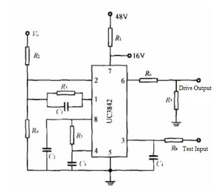
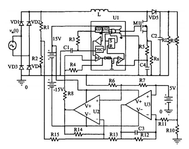
  3. UC3842 is a fixed frequency current-mode PWM controller. This IC is specially designed for Off-Line and DC to DC converter applications with minimum external components. In the blog today, we'll have a further discussion about the application of UC3842 in the boost conversion circuit. Boost Conversion Circuit Overview Boost converters can reduce the output current and the capacitance and volume of the output filter capacitor under a certain output power, and are widely used in switching power supplies and electronic ballasts. Commonly used control methods are voltage feedback control and current feedback control. Current feedback control can force the inductor current to track the reference current signal, which has the advantage of fast response. When working in continuous current mode (CCM), the Boost converter needs to introduce multiple feedback methods. When working in discontinuous current mode (DCM), the converter automatically shapes the input current, and has a natural zero-current turn-on characteristic, requires a small inductance value, simple control, and is suitable for low-power applications. At present, there are many researches on the CCM mode of Boost conversion circuit, and many circuit models have been established, and gratifying research results have been obtained; the research on DCM mode is mainly DC/DC circuit, and the research on DCM mode in AC/DC circuit Very little. Based on the requirements of low-power switching power supply with low cost and high cost performance, this paper uses the universal UC3842 chip to design a Boost conversion circuit, analyzes the working characteristics and design points of the DCM mode, and simulates the rationality of the designed circuit verification. There are 2 circuit models of boost converter in DCM mode, named spectively as: Mathematical Model of DCM Working Mode and Working Conditions of DCM Mode. For detailed explanation to these two models>> DCM Circuit Design Based on UC3842 DCM Circuit Design Based on Adder The DCM-type Boost circuit includes two control loops, namely a voltage loop and a current loop. Its function is to eliminate the grid current spikes, so that the input current becomes a sinusoidal shape and is in phase with the input voltage. For a single switching cycle, the current in each switching cycle is required to be proportional to the input voltage. If for some reason the output voltage increases or the output current increases, the pulse width modulator will change the pulse width of the drive signal, that is, the duty cycle D, so that the average voltage or peak current after the chopping will decrease. So as to achieve the purpose of power factor correction. The DCM circuit schematic diagram based on the adder is shown in Figure below. The voltage outer loop uses an adder to replace the multiplier circuit. The feedback voltage on the grid side is used to ensure that the current signal is a sinusoidal signal, and the output feedback voltage is used to ensure that the output voltage is a constant value. The two are synthesized by the adder U2. The output signal is sent to the error amplifier in the UC3842 current loop, compared with a given reference voltage, and the comparison result is sent to the current measurement comparator. The peak current signal L(t) of the inductor in the main circuit is sent to the current measuring comparator at the same time, the comparison result of the two is sent to the R input of the RS latch in the PWM, the clock signal output by the internal oscillating circuit is sent to the S input end of the RS latch in the PWM, which works together to control the opening and closing of the switch tube M1. The follow-up simulation and analysis of DCM mode circuit>> Conclusion This text summarizes the Boost conversion circuit design scheme based on UC3842 chip. By analyzing the circuit of Boost converter in DCM mode, the circuit model of Boost converter in DCM mode is established, and the duty cycle change rule in this mode and the critical conditions for entering CCM mode from DCM mode are studied. Using the universal PWM modulator UC3842 chip, a Boost conversion circuit based on the principle of addition is designed, and the correctness of the conclusions obtained is verified by simulation software. The circuit simulation results show that the designed DCM circuit can meet the requirement of the inductor current to follow the voltage waveform completely and achieve the purpose of improving the power factor. This research provides design ideas for the development of low-cost low-power switching power supplies.
  4. Hi everyone, Many of you may be interested in building electronics DIY kits. Building kits is one of fun and effective ways to learn electronics as well as soldering skill. The most classic and practical kit is LED clock kit for sure. Available clock kits in market provide basic clock features like time and alarm setting. However, if you are looking for a clock kit with more comprehensive functions, more challenging soldering process and larger space for creation, the following clock kit is definitely for you. Let’s take a look at the main functions and features: ⭐ Jumbo 4-digit LED display ⭐ Low power consumption ⭐ 12H/24H time format setting function ⭐ Date setting function, the maximum date is 31 Dec 2099 ⭐ Alarm time setting ⭐ With internal memory for storing alarm settings ⭐ The system keeps running normally for approximately 1 minute when power off ⭐ System reset function ⭐ Selectable power saving mode ⭐ Adjustable LED display brightness ⭐ Low power indication ⭐ With timer output port for controlling peripheral equipment ⭐ Two power input options: (1) external power input (5.5-2.5mm DC Jack): DC 3-5V Adaptor, OR (2) internal power input (Battery Solder Pads): 1.5V Battery Cell x 3 (Battery Not Included) The kit includes detailed instruction manual and assembly manual. Clock housing is NOT included but the main PCB comes with two mounting holes for assisting you to unleash your creativity through making your unique housing, turn it into a desk clock or hang it on the wall. Watch below YouTube videos for better understanding how it works: 【Introductory Video】 (https://youtu.be/OnLkW0r0Nmw) Besides “introduction”, this video shows the assembled clock with innovative handmade cylinder case (it is too boring to make traditional cuboid case), hope it will inspire you to design your own stunning one. 【Operation Demonstration】 (https://youtu.be/D0cj9z7fEIE) It demonstrates every function and setting of the clock. 【Assembly Guides and Tips】 (https://youtu.be/WLdr1t99Q0U) It tells you gentle remainders before building the clock. We provide as kit or fully assembled version. If you are interested, you may directly place order on ETSY shop 👉🏻 https://www.etsy.com/hk-en/listing/697326534/4-digit-led-clock-kit-diy-clock-kit?ref=listings_manager_grid Or you may visit our website for details 👉🏻 http://www.alien-1.com Retail and wholesale are welcomed! Please contact 👉🏻 enquiry@alien-1.com / alien1.enquiry@gmail.com for further information.
×
×
  • Create New...