

Bob Collin
-
Posts
5 -
Joined
-
Last visited
Content Type
Profiles
Forums
Events
Everything posted by Bob Collin
-
Another comparison article of NE5532, hope it helps. https://www.apogeeweb.net/circuitry/NE5532-comparisons.html
-
The most comprehensive comparison article of L293D and its similar models i could find on the internet, it's useful to me, hope it's helpful to guys as well. https://www.apogeeweb.net/circuitry/l293d-comparisons.html
-
Hey guys, this is Bob. Just saw this dope project and im trying to make a temperature measurement device follow this article, seems kinda complicated at first sight but im decided to give it a go lol https://www.apogeeweb.net/circuitry/AD590-temperature-sensor.html
-
Hey guys, this is Bob, in today's blog we'll discuss the difference between 1N4148, 1N4007, 1N5819. I. Brief Introduction to 1N4148, 1N4007, 1N5819 1N4148 is a fast switching diode. It is fabricated in planar technology, and encapsulated in hermetically sealed leaded glass SOD27 (DO-35) packages. 1n4007 is a PN junction rectifier diode. These types of diodes allow only the flow of electrical current in one direction only. So, it can be used for the conversion of AC power to DC. 1N5819 is a Schottky diode with 2 pins, a peak current of 25A, and an operating temperature range of -65°C~ +125°C. It is commonly used in high frequency applications like Inverters, DC-DC converters etc. II. 1N4148 vs 1N4007 General difference 1. 1N4148 and 1N4007 can be replaced with each other in case of general small current (below 100mA, reverse voltage below 100V) and unimportant occasions. 2. 1N4148 is a small current switch tube, with a voltage resistance of 100V. 3. 1N4007 is a rectifier tube, 1A-1000V. There are many types of substitute models. Application difference Generally speaking, we mostly use 1n4148 when using freewheeling diodes; Since it is a freewheeling diode, it is generally used on inductive loads, such as: buzzer, relay; Several factors we have to consider are: 1. How fast is the freewheeling diode? Just take an appropriate value; for example, MS level, US level, NS level? 2. What is the current of the freewheeling diode? Look at the DS manual, don't burn it out. 3. How high is the voltage of the freewheeling diode? Look at the DS manual, don't break it. Conclusion 1N4148: 100V reverse withstand voltage and 150mA average forward current, very suitable for ordinary rectification in general occasions. The reverse recovery time of 4nS is sufficient for most occasions. 1N4007: Maximum forward average rectified current, 1A maximum reverse withstand voltage, 1000V low reverse leakage current, 5uA (maximum) forward voltage drop, 1.0V maximum reverse peak current, 30uA, reverse recovery time 30us; 1N4148: Generally, IN4148 is used in weak current inductive loads, such as buzzer and other small current inductive loads; 1N4007: Generally used in large current loads, such as industrial load (relay), power supply load; The biggest difference between them is the current, voltage, and response speed. In a sense, 1N4007 can replace 1N4148, as long as the response speed is not too demanding, 1N4148 is destined to be used only on weak current low-current inductive loads. III. 1N4148 vs 1N5819 High frequency, low voltage, and high current characteristics are the differences between 1N5819 diodes and ordinary diodes. It is widely used in switching power supplies, frequency converters, drivers and other circuits for high frequency, low voltage, high current rectification, freewheeling, and diode protection. 1N5819 is characterized by ultra-fast speed (low switching loss), extremely low forward voltage drop (low voltage loss), but also low reverse withstand voltage, usually less than 60V, suitable for low-voltage (no higher than 12V) switching power supply. Another use of 1N5819 diode is to use its reverse characteristic to stabilize voltage. Therefore, when the withstand voltage is low and the current is not large, you can consider using a Zener tube instead. 1N4148 is a point contact type low current high frequency switching diode with high speed, but the working current is only 150mA, which is widely used in circuits with higher signal frequencies. The reverse leakage of 1N5819 tube is relatively large, but it has the characteristics of small capacitance and high speed. But it is not as fast as 1N4148, after all, the purpose of 1N4148 is high frequency detection, not rectification.
-
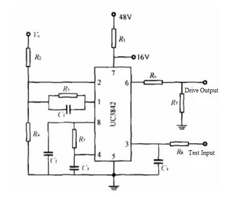
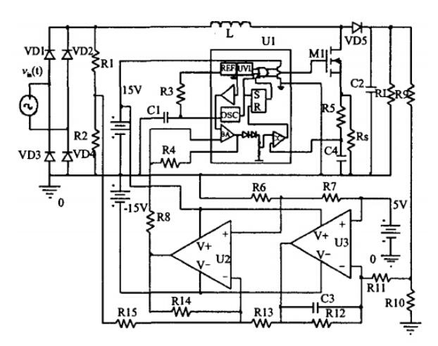
UC3842 is a fixed frequency current-mode PWM controller. This IC is specially designed for Off-Line and DC to DC converter applications with minimum external components. In the blog today, we'll have a further discussion about the application of UC3842 in the boost conversion circuit. Boost Conversion Circuit Overview Boost converters can reduce the output current and the capacitance and volume of the output filter capacitor under a certain output power, and are widely used in switching power supplies and electronic ballasts. Commonly used control methods are voltage feedback control and current feedback control. Current feedback control can force the inductor current to track the reference current signal, which has the advantage of fast response. When working in continuous current mode (CCM), the Boost converter needs to introduce multiple feedback methods. When working in discontinuous current mode (DCM), the converter automatically shapes the input current, and has a natural zero-current turn-on characteristic, requires a small inductance value, simple control, and is suitable for low-power applications. At present, there are many researches on the CCM mode of Boost conversion circuit, and many circuit models have been established, and gratifying research results have been obtained; the research on DCM mode is mainly DC/DC circuit, and the research on DCM mode in AC/DC circuit Very little. Based on the requirements of low-power switching power supply with low cost and high cost performance, this paper uses the universal UC3842 chip to design a Boost conversion circuit, analyzes the working characteristics and design points of the DCM mode, and simulates the rationality of the designed circuit verification. There are 2 circuit models of boost converter in DCM mode, named spectively as: Mathematical Model of DCM Working Mode and Working Conditions of DCM Mode. For detailed explanation to these two models>> DCM Circuit Design Based on UC3842 DCM Circuit Design Based on Adder The DCM-type Boost circuit includes two control loops, namely a voltage loop and a current loop. Its function is to eliminate the grid current spikes, so that the input current becomes a sinusoidal shape and is in phase with the input voltage. For a single switching cycle, the current in each switching cycle is required to be proportional to the input voltage. If for some reason the output voltage increases or the output current increases, the pulse width modulator will change the pulse width of the drive signal, that is, the duty cycle D, so that the average voltage or peak current after the chopping will decrease. So as to achieve the purpose of power factor correction. The DCM circuit schematic diagram based on the adder is shown in Figure below. The voltage outer loop uses an adder to replace the multiplier circuit. The feedback voltage on the grid side is used to ensure that the current signal is a sinusoidal signal, and the output feedback voltage is used to ensure that the output voltage is a constant value. The two are synthesized by the adder U2. The output signal is sent to the error amplifier in the UC3842 current loop, compared with a given reference voltage, and the comparison result is sent to the current measurement comparator. The peak current signal L(t) of the inductor in the main circuit is sent to the current measuring comparator at the same time, the comparison result of the two is sent to the R input of the RS latch in the PWM, the clock signal output by the internal oscillating circuit is sent to the S input end of the RS latch in the PWM, which works together to control the opening and closing of the switch tube M1. The follow-up simulation and analysis of DCM mode circuit>> Conclusion This text summarizes the Boost conversion circuit design scheme based on UC3842 chip. By analyzing the circuit of Boost converter in DCM mode, the circuit model of Boost converter in DCM mode is established, and the duty cycle change rule in this mode and the critical conditions for entering CCM mode from DCM mode are studied. Using the universal PWM modulator UC3842 chip, a Boost conversion circuit based on the principle of addition is designed, and the correctness of the conclusions obtained is verified by simulation software. The circuit simulation results show that the designed DCM circuit can meet the requirement of the inductor current to follow the voltage waveform completely and achieve the purpose of improving the power factor. This research provides design ideas for the development of low-cost low-power switching power supplies.